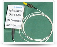
|
Min |
Typical |
Max |
Positive supply voltage (V) |
4.75 |
5 |
5.25 |
Avalanche Photo Diodeˇ¦s HV Supply |
|
Internal |
Power consumption (W) |
|
1.7 |
2.5 |
Output data & clock voltage
single ended (Vpp)
|
|
0.4 |
0.8 |
Output data & clock voltage
differential (Vpp)
|
|
0.8 |
1.6 |
Output rise time 20 % to 80 % (ps) |
|
|
150 |
Output fall time 80 % to 20 % (ps) |
|
|
150 |
Data output jitter p-p (ps) |
|
|
20 |
Output clock & data return loss |
Clock 1 to 2 GHz (dB): |
6 |
Clock 2 to 2.8 GHz (dB): |
12 |
Data 1 to 1 GHz (dB): |
12 |
Data 1 to 2 GHz (dB): |
9 |
Data 2 to 2.5 GHz (dB): |
6 |
Loss of Power Alarm output level normal signal (V): |
0 |
|
0.4 |
Loss of power alarm output level: low signal input (alarm): |
2.4 V |
|
Vcc |
ˇ§Low Lightˇ¨ alarm assert time (ms): |
|
|
1 |
ˇ§Low Lightˇ¨ alarm de-assert time (ms): |
|
|
1 |
Clock and data differential skew (ps): |
|
|
20 |
Clock duty cycle |
45 % |
|
55 % |
Maximum receives clock frequency drift
with no light input (MHz):
|
|
|
100 |
Data, clock load drive capability is Externally AC coupled, terminated into 50 ohms. |
Consecutive identical bits |
|
|
72 bits |
Jitter generation |
Meets GR-253/ITU-T G.958 |
Jitter tolerance |
Meets GR-253/ITU-T G.958 |
Jitter transfer |
Meets GR-253/ITU-T G.958 |
Logic output level TTL compatible |